
By Johnny Quest

All posts in ascending order.

01: Another Z80 single-board computer?
02: Initial design criteria
03: Working on the SPLD to use as an I/O decoder
04: Testing the 74HC299 data bus interface
05: Testing the AVR’s interrupt latency.
06: 1st attempt at a programmable wait-state generator
07: Moving the programmable wait-state generator into a GAL22V10
08: Programming the memory and I/O address decoder PLD
09: More testing of the memory and I/O address decoder PLD
10: Getting the Z88DK software development suite up and running
11: Z80 testing – Simple program to exercise the UART
12: Progress Update
13: PC Board artworks off to the fabricator
14: Success with FAT library !
15: Project goals as thoughts and concepts now put into words …
16: Additional thoughts on “debugging” Z80 code on the Z80 SBC.
17: Project Reference: A “Modern Day” Z80 Hardware Emulator
18: Update: Investigation into Z80 real-time debugging on the AVR
19: PCB arrival – initial hardware check
20: Hardware test – 2nd phase
21: Update for March 17, 2017
Update for March 17, 2017
I realized that the last post on this project was nearly two months ago, so here’s an update.
The project is still alive! I’ve had other projects that took some time away from me for the time being.
I have performed some more hardware testing on the Z80 SBC using AttoBASIC. I wrote a small Z80 program and loaded it into RAM for the Z80 to run and it works as expected. The program is simple, stuff some bytes to the AVR’s I/O port address and do the same for the 82C55’s I/O port address. The intention was to be able to test the I/O port decoding in the ATF16V8 PLD and test the programmable wait-state generator, which is triggered by the Z80’s access to the AVR’s I/O address. These functions work as expected and I will post on that later.
Meanwhile, I am still mulling over which software development method to use for the AVR host. Although I have written code for one project in “C”, I am not “C” fluent, thus I am leaning towards pure assembly language, which I am quite comfortable developing in. Even so, there are some pros and cons to using “C” or ASM.
Using “C”:
- Not fluent, thus steep learning curve (again) to implement and comprehend the nuances of “C” on the AVR.
- SDcard library is written in “C”, so easier to interface with.
- DS3231 RTC library is written in “C”, so easier to interface with.
Using ASM:
- Very fluent, no learning curve.
- Can use AttoBASIC as a starting point but that requires deletion of most commands, addition of Z80-specific commands and modification to some of the existing commands, including support for 16-bit numbers as parameters. I have already done this for another project and it supports 32-bit numbers as parameters to the commands. Still, its a bit of a task and I would not merge this into the AttoBASIC source code.
- Interface to the SDcard library requires reverse engineering the resulting ASM code, determining library API absolute addresses and the absolute locations of data in RAM. I’ve done this before BUT the SDcard library uses a lot of local variables and internal management.
- Interface to the DS3231 library requires reverse engineering the resulting ASM code, determining library API absolute addresses and the absolute locations of data in RAM. However, the DS3231 interface is simple enough that it would be easier to write my own code for it.
So that’s it in a nutshell.
Stay tuned as I am making progress.
Peace and blessings.

Hardware test – 2nd phase
With the PCB’s in and the initial hardware check finished and me delaying far too long on getting back to this project, it was time to move on to verifying that my intended hardware functionality did, in fact, work as planned. There are several functional blocks that need to be tested, both on the AVR and the Z80 support circuitry.
For this post, I’ll focus on three specific functional blocks:
- AVR as the Z80 system clock
- AVR interface with the DS3231 RTC module
- AVR interface with the system, data and address buses
On past projects, especially when acquiring and evaluating various OEM samples to be used with a microcontroller, I’ve always found it time consuming to write different test programs over and over again. Always having to configure, reconfigure, flash, test, debug, fix code, re-flash and do it all over again. Those real-time debug cycles on any FLASH-based MCU can be very time consuming, which I sought out ways to cut the time. To that end, I ran across Dick Cappels‘ AttoBASIC back in 2011. With some modifications to the code, I was able to fully support the TWI and SPI interfaces for the project I was working on at the time. Since then, I have found it to be indispensable in evaluating new hardware devices and initial hardware testing when an AVR is the embedded microcontroller on a particular project, such as this Z80 SBC. It also helps to be the AttoBASIC maintainer (since 2011) as I know the program well enough to add support for any feature if I find I have a need for it. For the following initial hardware testing, I have been using AttoBASIC and to provide others with examples, I will provide each program listing that was used for the testing.
With all the I/O ports that the ATMEL AT90USB1286 provides, I still found myself a little bit shy in ports. I wanted to leave the JTAG interface and some A/D channels available, thus PORTF was not fully accessible. I ended up using a 74HC299 to interface to the Z80 databus. The 74HC299 is an “8-bit universal shift register with 3-state outputs“. Its a nice part that comes in a 20-pin package. I chose to use the DIP package for this project. From the 74HC299 datasheet:
The 74HC299; 74HCT299 contain eight edge-triggered D-type flip-flops and the
interstage logic necessary to perform synchronous shift-right, shift-left, parallel load and
hold operations. An operation is determined by the mode select inputs S0 and S1, as
shown in Table 3.

Pins I/O0 to I/O7 are flip-flop 3-state buffer outputs which allow them to operate as data
inputs in parallel load mode. The serial outputs Q0 and Q7 are used for expansion in
serial shifting of longer words.
1st test, Z80 clock: I had already tested this function on my breadboard using an assembly language program but that was with an ATmega328P. It should work the same on the AT90USB1286 but I wanted to be sure … and it did. Its a simple program; initialize all ports to their proper state, setup TIMER 2 as the Z80 clock source and generate a pulse on the Z80 CLK RST pin. The majority of the program listing is for documentation. Here’s the AttoBASIC program listing:
5 REM Z80 POWER-UP INIT
10 REM PD2=IORQ, PD3=MREQ, PD4=WR, PD5=RD
15 REM PF1/PF0 = S1/S0 FOR WS-GEN
20 REM PB0=HC299_CS, PB6=HC299_OE, PB7=HC299_S1
25 REM PB4=Z80CLK, PE2=Z80RST, PD6=Z80BUSRQ
30 OPA $FF, OPC $FF         # SET ADDRESS PORT AS INPUTS W/ PUPS (C=A[15:8], A=A[7:0])
35 OPB $D0; ODB $D0         # SET PORTS
40 OPD $FF; ODD 0           # SET PORTS
45 OPE $F3; ODE $04         # SET PORTS
50 OPF $00; ODF $03         # SET PORTS
55 REM SETUP TMR2: TCCR2A(@$B0)=$42, TCCR2B(@$B1)=$01, OCR2A($B3)=$07
60 X:= PEEK 0 $64; X:= X AND $BF; POKE X 0 $64      # TMR2 ENABLE IN PRR0
65 POKE $3F 0 $B3; POKE $42 0 $B0; POKE $01 0 $B1   # SETUP TMR2 AS 125KHZ Z80 CLK
70 PBE2                                             # GENERATE A RESET PULSE TO CYCLE REGISTERS
75 END
2nd test, RAM R/W test: To test the address, data and system control buses, I initially wrote a program to set the AVR’s I/O ports, then with the Z80 removed from the circuit, I wrote data to the RAM, read the data back from the RAM, incremented the address bus and repeated the cycle for all 65,536 bytes of RAM. I then decided to expand upon that by testing the RAM with the Z80 in-circuit. After all, that will be the final goal, to use the AVR as a host controller with the Z80 in-circuit. Below is the logic analyzer’s capture of the AttoBASIC program that is testing RAM. What is important to note here is that in testing the memory, I am also testing the AT16V8 address decoder.
I only have 16 channels available on my logic analyzer so I chose to capture the Z80’s DATA[7:0], ADDR[2:0], RD, WR, MREQ, BUSREQ and BUSACK, triggering on the falling edge of the BUSACK signal. In doing so, I could test that the Z80 responds to a request for the bus, relinquishes the bus and acknowledges it. During the test, the Z80’s clock was active and a reset pulse was applied before dropping the BUSREQ line and waiting for the BUSACK line to drop active low. Once BUSACK was detected low, the program proceeded to sequentially test each RAM location. The address can be seen incrementing and although the scale is too large to see the contents of the data bus, a 0x55 is being written and read back then complimented so that a 0xAA is written and read back from the next location. The state of the MREQ, RD and WR lines can also be seen.
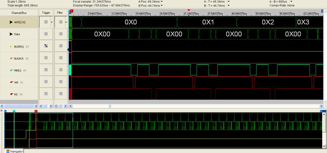
RAM Test w/ AttoBASIC
I would not say that AttoBASIC was speedy when it came to testing, as sequential memory accesses took about 15.88 mS, which was about 63 bytes per second. As calculated, it would take 17 minutes and 19.4 seconds to complete the test if there were no errors to report. In actuality, the AttoBASIC program reported that it took 17 minutes and 9.3 seconds to complete and there were no errors. However slow it may be compared to pure assembly or “C” code, it served it’s purpose. The AttoBASIC program code is listed below:
5 REM Z80 RAM ERROR TEST
10 REM PD2=IORQ, PD3=MREQ, PD4=WR, PD5=RD
15 REM PB4=Z80CLK, PE2=Z80RST, PD6=Z80BUSRQ
20 REM PF1/PF0 = S1/S0 FOR WS-GEN
25 REM PB0=HC299_CS, PB6=HC299_OE, PB7=HC299_S1
30 SPM 2# SPI TO MODE 2
35 D:= $55; Z:=0                  # DATA TO WRITE=$55, Z HOLDS '0'
40 GOSUB 220                      # INSURE ALL PORTS AS INPUTS
45 GOSUB 225                      # START Z80 CLOCK AND INITIATE A Z80 RST
50 SDD6; CBD6                     # INITIATE Z80 BUSRQ
55 IF 1 = IBE0                    # WAIT FOR Z80 BUSACK
60 GOTO 55                        # LOOP TILL Z80 BUSACK
65 ODA $FF; OPA $00               # SET PORTA OUTPUT AND ADDRESS A[7:0] =0x00
70 ODC $FF; OPC $00               # SET PORTC OUTPUT AND ADDRESS A[15:8] =0x00
75 OPB '11010001; ODB '11010111   # SS=1 (SEL HC299), OE=1 (HI-Z), (S0=1/S1=1)
80 ODD '11111100; OPD '10111111   # CONTROL PORT TO OUTPUTS, ALL HIGH
85 ODE '00000100; OPE '11111111   # SET PORTE, INPUTS W/ PULL-UPS
90 ODF '00000011; OPF '11111100   # SET S0/S1 OUTPUTS FOR 0 WS
95 RTI 2; RTR                     # SET 100MS RTC INTERVAL AND RESET THE RTC
100 FOR U=0 255; FOR L=0 255      # SET UP THE UPPER AND LOWER ADDRESS LOOPS
105 OPC U; OPA L                  # OUTPUT CURRENT ADDRESS ONTO BUS
110 GOSUB 165                     # WRITE DATA TO THE RAM ADDRESS
115 GOSUB 180                     # READ DATA FROM THE RAM ADDRESS AND PRINT IT
120 SBD5; SBD3                    # RAISE THE Z80 RD AND MREQ SIGNAL
125 IF X != D                     # RESULT = EXECTED?
130 GOSUB 195                     # ERROR, INFORM USER
135 D:= COM D                     # COMPLIMENT DATA TO WRITE (ODD/EVEN ADDR)
140 NEXT L; NEXT U                # CONTINUE INCREMENT LOOP
145 PRI PEEK VPG@RTC1; PRI PEEK VPG@RTC0  # PRINT THE CONTENTS OF THE RTC (IN 0.1 SEC)
150 ODA $FF; ODB $FF; ODC $FF; ODD $FF    # SET ALL PORTS TO INPUTS
155 END
160# *** WRITE DATA TO DATA BUS ***
165 CBB7; SPW D; CBB6; CBD3            # SHIFT ENABLE, WRITE DATA='D', ENABLE DATA ONTO                                                                                   #  BUS, DROP Z80 MREQ
170 CBD4; SBD4; SBD3; SBB6; SBB7; RET  # PULSE Z80 WR, RAISE Z80 MREQ, OE=1,S1=1 THEN RETURN
175# *** READ DATA FROM DATA BUS ***
180 CBD3; CBD5; SPW 0; SBD5; SBD3      # DROP Z80 MREQ, DROP Z80 RD, DUMMY WRITE TO                                                                                            # LOAD, RAISE Z80 RD, RAISE Z80 MREQ
185 CBB7; X:= SPR; SBB7; RET           # S1=0, 'X'=READ DATA, S1=1 THEN RETURN
190# *** PRINT ERROR MESSAGE *** ;
195 PRI "ERROR DETECTED AT:~"          # INFORM USER OF ERROR IN TESTING
200 PRI "A[15:8]="; PRX U              # INFORM USER OF UPPER ADDRESS
205 PRI "A[ 7:0]="; PRX L              # INFORM USER OF LOWER ADDRESS
210 PRI "EXPECTED= "; PRX D; PRI "RESULT = "; PRX X
215 PRINT "~"; RET                     # INSERT CR/LF BETWEEN ADDRESSES
220 ODA Z; ODB Z; ODC Z; ODD Z; ODE Z; ODF Z; RET   # ALL PORTS TO INPUTS
222 REM SETUP TMR2: TCCR2A(@$B0)=$42, TCCR2B(@$B1)=$01, OCR2A($B3)=$07
225 X:= PEEK 0 $64; X:= X AND $BF; POKE X 0 $64     # TMR2 ENABLE IN PRR0
230 SDB4; POKE 63 0 $B3; POKE $42 0 $B0; POKE 1 0 $B1  # SETUP TMR2 AS 1MHZ Z80 CLK
235 SDE2; SBE2; PBE2; RET              # GENERATE A RESET PULSE TO CYCLE REGISTERS AND RETURN
DS3231 RTC test: The AVR is directly connected to the DS3231 RTC via the I2C (TWI) bus. I had already written a program to interface with a TEXAS INSTRUMENTS bq32000, which is also a real-time clock with a nearly identical register set as the DS3231. It took only a slight modification to that program and I was able to test the DS3231. The program sets the date and time to a set value, waits 4 second, reads it back again and displays the result. The AttoBASIC program code is listed below:
5 REM DS3231 RTC TEST
10 TWI 1                               # INIT TWI @100kbps
15 A:= $D0 ; B:= $D1                   # WRITE AND READ ADDRESSES FOR BQ32000 RTC
20# *** CONFIGURE THE DS3231
25 TWS ; TWW A $E 0; TWP               # write config register
30# *** INITIALIZE TIME AND DATE DATA TO RTC REGISTERS
35 DATA $00 $00 $60 $00 $22 $12 $16    # setup RTC's time and date
40 FOR Z=0 6                           # set data registers 0 to 6
45 R:=Z ; D:= READ                     # set register and data
50 TWS; TWW A R D; TWP                 # Write data to a register
55 NEXT                                                                   # end of loop
60# *** WAIT A BIT FOR THE SECONDS TO CHANGE THEN READ THE REGISTERS BACK
65 PRINT "Wait 4 sec~" ; SLP 8         # wait 4 seconds to see if the clock is running
70 TWS; TWW A 0                        # Select register 0, no STOP
75 TWS; TWW B; TWR 7; TWP              # slave to read and retrieve 7 bytes
80# *** LOOP AND PRINT EACH REGISTER'S VALUE
85 FOR R=0 6                           # Loop from register 0 to 6
90 PRINT "R:" ; PRI R                  # print the register
95 PRINT "D=" ; PRX READ               # print the data in the register
100 NEXT                               # end of loop
105 END
I did not test the wait-state generator as it was previously tested on the breadboard circuit, thus I already know it works.
An additional note: the overall current consumption is measured at ≈250 ma.
This completes the testing of the major functional blocks on the Z80 SBC. The next phase is to start writing the AVR host controller firmware.
Peace and blessings.

PCB arrival – initial hardware check
The Z80 SBC PCB’s finally arrived. They were shipped only 3 days after the 8052 SBC PCB’s but arrived 10 days later. Go figure …
When I was able to sit down and start the build process, I set out to populate and solder a test and development unit. One of the 1st issues I had run across a week ago was discovered, er, uh, realized in a “duh moment” … the pinout for the SD memory card module was reversed from what I had intended. I had originally defined the layout symbol looking from the top-down (component side) orientation, which was fine if I had mounted it on the component side of the PCB but I didn’t. The layout package I am using allows me to “flip” (mirror) the symbol to to bottom side of the PCB layout but in doing so, it also mirrors the pad orientation, which I did not think about at the time. My intention was to nestle the components between the SD memory card module and the bottom of the Z80 PCB, thereby protecting them. I should have constructed another symbol that reversed the pads to use for that purpose but I did not. So what I have to do is mount the SD memory card reader PCB with the components facing out. Not a big deal but ideally, not what I had wanted.
In case there was any rework to be done, the SD memory card module may be in the way, so I decided to leave it off the board for the time being, I have two different types of 40-pin IC sockets. One is a solid plastic frame with no voids in it and the other was a “frame” with voids in the frame so that you can see the PCB under it when the IC is removed from the socket. It was always my intention to use the “open frame” socket for the Z80 since that’s where the SD memory card’s solder pads are located and I figured it to better to be able to get at them than not. However, after the build, I realized that I used the “solid frame” socket type for the Z80. Oops! In my haste, I had forgotten to use the “open frame” socket. I had to desolder all 40 pins and gently lift the 40-pin socket out of the solder holes, hoping NOT to rip any through hole plating or traces up in the process. [The two different socket types can be seen in the reference photos below as well as the removed frame support between pin 20 and 21] All pins and pads seemed clear but after removing the socket, I saw that I had fully ripped the top solder pad off of pin 39 and the single 6 mil trace going to it … and partially ripped the top solder pad off of pin 10 and one of the two 6 mil traces going to it. The rework wasn’t to bad after it was completed. Reference “C” in the photos below.
In mounting the TEENSY module, I found that the E4 and E5 connections were skewed off by 50 mils. I am not sure how that happened because I measured those distances as I was creating the PCB foot-print. Since I used the thin excess lead clippings from the 100 nF capacitors for the connections to the Z80 PCB, the 50 mil difference wasn’t an issue. If it was off by more than 50 mils, it likely would have been.

PCB mods, top clad

PCB mods, bottom clad
With those pre-power-up mods out of the way, I proceeded to check the power supply input from power applied via the external power plug, since it powers all circuitry except the TEENSY. In case there was too much current draw from the USB port, which is required for the USB-to-serial interface, I added a means to supply external power via a “standard” 2.1/6 mm “power socket”. I found there was no power to the LM7805 voltage regulator and when I investigated the power socket, I found that the “tip and sleeve” connections were reversed. Since there is a 1N4001 diode in series with the input to the LM7805, there was no electrical damage. I do not recall actually checking that the schematic symbol and PCB symbol matched before submitting the GERBER files to the PCB fab house and that was the problem. I had to cut the thermal reliefs from the “tip” connection to ground and scrape off some solder mask to access the ground plane for the “sleeve” connection but it was a fairly quick fix. Reference “A” in the photos above.
Once the power socket issue was corrected, I could see that I had 5 volts to the logic supply rails. The TEENSY derives it’s power from the USB socket (the “USB_VCC” net) but I added a high-side P-MOSFET (Si2305) and a simple “external power detection” to act as a “switch-over circuit”. The circuit supplies 5 volts from the TEENSY/USB connection to the rest of the components (via the Si2305) unless there is external power applied, at which time it breaks the TEENSY’s power connection to the rest of the components. The voltage difference between the USB power and the 5 volt regulator is only about 200 millivolts, so as long as the TTL levels are met then there should be no unforeseen issues using this method. However, I could see that with the TEENSY powered up, the USB power was not getting to the rest of the components. I knew I had run the circuit through LINEAR TECH’s free “LTspice IV” circuit simulator and it worked. After some investigation, I looked at the pinout of the Si2305 datasheet, the schematic symbol and the PCB layout symbol and saw that pins 2 and 3 were reversed on the schematic symbol. The Si2305 is one of two SMT devices on this PCB. The Si2305 is housed in a (3 pin) SOT-23 package. Luckily, pins 2 and 3 are on the same side of the component, so flipping the SOT-23 over, bending the pins back and resoldering them to the PCB solved that problem. The “switch-over circuit” was now functioning properly. It is difficult to see behind the TEENSY but reference “D” in the photos above.
With the power-supplies functioning correctly, I decided to check for proper communication with the TEENSY via the JTAG header. I am using the JTAG header because the ATMEL AT90USB1286 “on-chip debugger” can only be accessed via the JTAG interface, not the ISP interface. I much prefer to use the JTAG interface for on-chip debugging over the debug-wire interface because then JTAG interface is MUCH more reliable that the debug-wire interface. Sometimes the debug-wire interface can unexpectedly abort and will not reconnect, which leaves the AVR in a state that it cannot be communicated with unless the debug-wire fuse is disabled and the SPI interface is re-enabled and most times that requires an HVPP (or HVSP) connection to do so. However, newer versions of avrdude (6.0+) recognize this and temporarily sets the MCU into a state that the fuses can be re-programmed using the SPI connection.
Continuing, a simple query of the AT90USB1286 by avrdude yielded a “RSP_NO_TARGET_POWER” response. I checked pin 4 (VTRef) of the JTAG connector and it had no power. In looking at the PCB layout program, I could see there were traces between pins 4 and 7 (VSup) but not to Vcc. Well, that was the problem. Looking at the schematic, I could see that I had labeled those two pins as connecting to the “VDD” net but all the other components were connected to the “VCC” net. I had copied that particular component and it’s connections from another schematic and failed to rename the “VDD” net to “VCC”. Since some pre-made schematic symbols use the “VDD / VSS” nets for the power pin(s) and others use the “VCC / GND” nets for the power pin(s), I usually connect the “VDD / VCC” and “VSS / GND” nets together in my schematics. I failed to connect the “VDD” and “VCC” nets together in this schematic. Another simple fix as there was a VCC connection available on the neighboring 74HC14 at pin 14. Reference “E” in the photos above.
With JTAG power restored, I still was unable to communicate with the AT90USB1286 on the TEENSY module. After pondering about it for a few minutes, I considered the possibility that during the OEM’s programming of the PJRC “Half-Kay” boot-loader, perhaps the JTAG interface was disabled in the fuse programming. The only way to find out was to temporarily wire in an ISP connection and talk to the AT90USB1286 using the ISP interface. I had NEVER intended to use an ISP connection to the TEENSY because I wanted to use the on-chip debugger for code development, which is JTAG. In addition, the SPI connections are being used to communicate with the SD memory card and the 74HC299. The MISO connection from the SD memory card and the “QH” connection from 74HC299 are individually routed to the SPI port via a “pico-gate” MUX (NC7SP157, a single 74HC157-type MUX), which uses the “SS” (slave-select) signal from the SPI port to select between the two. It should, however, be easy enough to wire in the SPI connections to my AVR DRAGON but with the MUX driving the MISO signal, I’d have to connect to the SD memory card’s MISO pad to get through the MUX to the AT90USB1286. Well, I tried that and it still did not work. Then I realized that in SPI programming mode, the MISO/MOSI connections are reversed from that of the “normal” SPI operations as the AVR becomes the “slave”. The ONLY way to overcome this (hopefully) one-time operation was to cut the trace to the MISO pin at the TEENSY and reconnect it afterwards. A few minutes later and I had a successful ISP connection to the AT90USB1286 and yes, the JTAG interface was disabled. The only way to reset the fuses was to erase the AT90USB1286’s FLASH memory and thereby the “Half-kay” boot-loader. I had always intended to use Dean Camera’s(open-source) LUFA CDC boot-loader, so wiping out the (closed-source) “Half-Kay” boot-loader wasn’t a problem for me. A few minutes later and I had the JTAG interface working again and the cut trace restored. Reference “B” in the photos above.
BTW: Since there are 2 SMT components on the Z80 PCB and the NC7SP157 is housed in a 6-pin SC-70 package, it was easier to use my “home-brew” reflow oven to affix them to the PCB rather than breaking out my fine-tipped soldering iron. Using the larger tipped soldering iron would not have been a problem for the SOT-23 package but the for the SC-70 package, the pins are spaced too closely to even want to try.
With my initial issues overcome, it was time to start testing the hardware with the TEENSY. I’ll load AttoBASIC and use it to functional test each hardware block. Look for the results in the next entry.
